Cmos Nand Gate Schematic Explained Transistor Level Design Working Simulation In Vlsi Information Center
Get comprehensive updates, key reports, and detailed insights compiled from verified editorial sources.
About to Cmos Nand Gate Schematic Explained Transistor Level Design Working Simulation In Vlsi

Description: Welcome to TMSY Tutorials, your trusted platform to learn Description: Welcome to TMSY Tutorials – your one-stop destination for learning This video provides a basic introduction into logic In this video, we design a CMOS 3-Input NAND Gate schematic step by step using basic VLSI concepts. This tutorial is perfect ... Description: Welcome to TMSY Tutorials, your ultimate learning hub for Description: Welcome to TMSY Tutorials – your go-to channel for mastering
Core Information

Explore the main sources for Cmos Nand Gate Schematic Explained Transistor Level Design Working Simulation In Vlsi.
Latest News

Stay updated on Cmos Nand Gate Schematic Explained Transistor Level Design Working Simulation In Vlsi's latest milestones.
Featured Video Reports & Highlights
Below is a handpicked selection of video coverage, expert reports, and highlights regarding Cmos Nand Gate Schematic Explained Transistor Level Design Working Simulation In Vlsi from verified contributors.
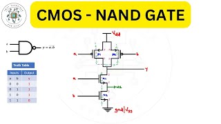
CMOS NAND Gate Schematic Explained | Transistor-Level Design, Working & Simulation in VLSI

CMOS NAND Gate
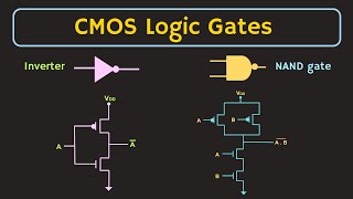
CMOS Logic Gates Explained | Logic Gate Implementation using CMOS logic
Full Guide
Data is compiled from public records and verified media reports.
Last Updated: May 22, 2026
Conclusion

For 2026, Cmos Nand Gate Schematic Explained Transistor Level Design Working Simulation In Vlsi remains one of the most talked-about profiles. Check back for the latest updates.
Disclaimer:


![What is a CMOS? [NMOS, PMOS]](https://i0.wp.com/ytimg.googleusercontent.com/vi/docgmTprR5o/mqdefault.jpg?resize=320,180)


