Gate All Around Transistor Architecture Designed For The Future Of Logic Devices Semi 101 Information Center
Get comprehensive updates, key reports, and detailed insights compiled from verified editorial sources.
About of Gate All Around Transistor Architecture Designed For The Future Of Logic Devices Semi 101

Applied Materials engineers have been working with our customers for many years to develop the key materials engineering ... What are GAAFETs and how does their shape change the Links: - The Asianometry Newsletter: - Patreon: - Threads: ... We take a look at the fundamentals of how computers work. We start with a look at Learn more about Intel's Process and Packaging Innovations: At its "Intel Accelerated" event on July 26, ...
Key Details
Explore the key sources for Gate All Around Transistor Architecture Designed For The Future Of Logic Devices Semi 101.
Developments

Stay updated on Gate All Around Transistor Architecture Designed For The Future Of Logic Devices Semi 101's latest milestones.
Featured Video Reports & Highlights
Below is a handpicked selection of video coverage, expert reports, and highlights regarding Gate All Around Transistor Architecture Designed For The Future Of Logic Devices Semi 101 from verified contributors.
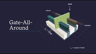
Gate-All-Around, Transistor Architecture Designed for the Future of Logic Devices (Semi 101)

Engineering the Gate-All-Around Transistor
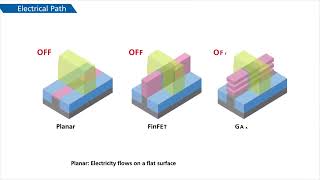
GAA (Gate-All-Around) Transistor

Gate-All-Around — The Future of Transistors
Deep Dive
Data is compiled from public records and verified media reports.
Last Updated: May 24, 2026
Conclusion

For 2026, Gate All Around Transistor Architecture Designed For The Future Of Logic Devices Semi 101 remains one of the most talked-about profiles. Check back for the newest reports.
Disclaimer:


