Measuring Stress In 7nm Finfets Information Center
Get comprehensive updates, key reports, and detailed insights compiled from verified editorial sources.
About of Measuring Stress In 7nm Finfets

This video dives into the invisible but critical role of mechanical ANSYS' Karthik Srinivasan talks with Semiconductor Engineering about the effect of heat on reliability at advanced process nodes ... GlobalFoundries' Jamie Schaeffer talks with Semiconductor Engineering about 22nm and 12nm FD-SOI and what the tradeoffs ... Randy Caplan, Executive VP at Silicon Creations discusses high performance PLL design in 5nm at DAC 2018. Device scaling for sub-10 nm CMOS technology has introduced bulk/SOI Victor M. van Santen, Hussam Amrouch, Poja Sharma and Jörg Henkel: "On the Workload Dependence of Self-Heating in
In keeping with Moore's Law, discover how Synopsys is developing 10nm/ Ana Hunter, VP Foundry, Samsung Semiconductor -- 14nm
Core Information

Explore the primary sources for Measuring Stress In 7nm Finfets.
Latest News
Stay updated on Measuring Stress In 7nm Finfets's latest milestones.
Featured Video Reports & Highlights
Below is a handpicked selection of video coverage, expert reports, and highlights regarding Measuring Stress In 7nm Finfets from verified contributors.
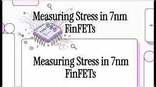
Measuring Stress in 7nm FinFETs
SForum 2020 - Design and Robustness Evaluation of a 7nm FinFET DICE SRAM

7nm Thermal Effects (2017)

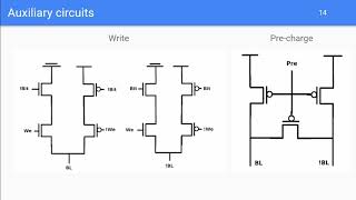
7nm FINFET Layout
Full Guide
Data is compiled from public records and verified media reports.
Last Updated: May 22, 2026
Summary

For 2026, Measuring Stress In 7nm Finfets remains one of the most searched-for profiles. Check back for the newest reports.
Disclaimer:


![[Electronics] High-resolution Cut & See of 10 nm FinFET](https://i0.wp.com/ytimg.googleusercontent.com/vi/SrZsJLT8rSI/mqdefault.jpg?resize=320,180)


